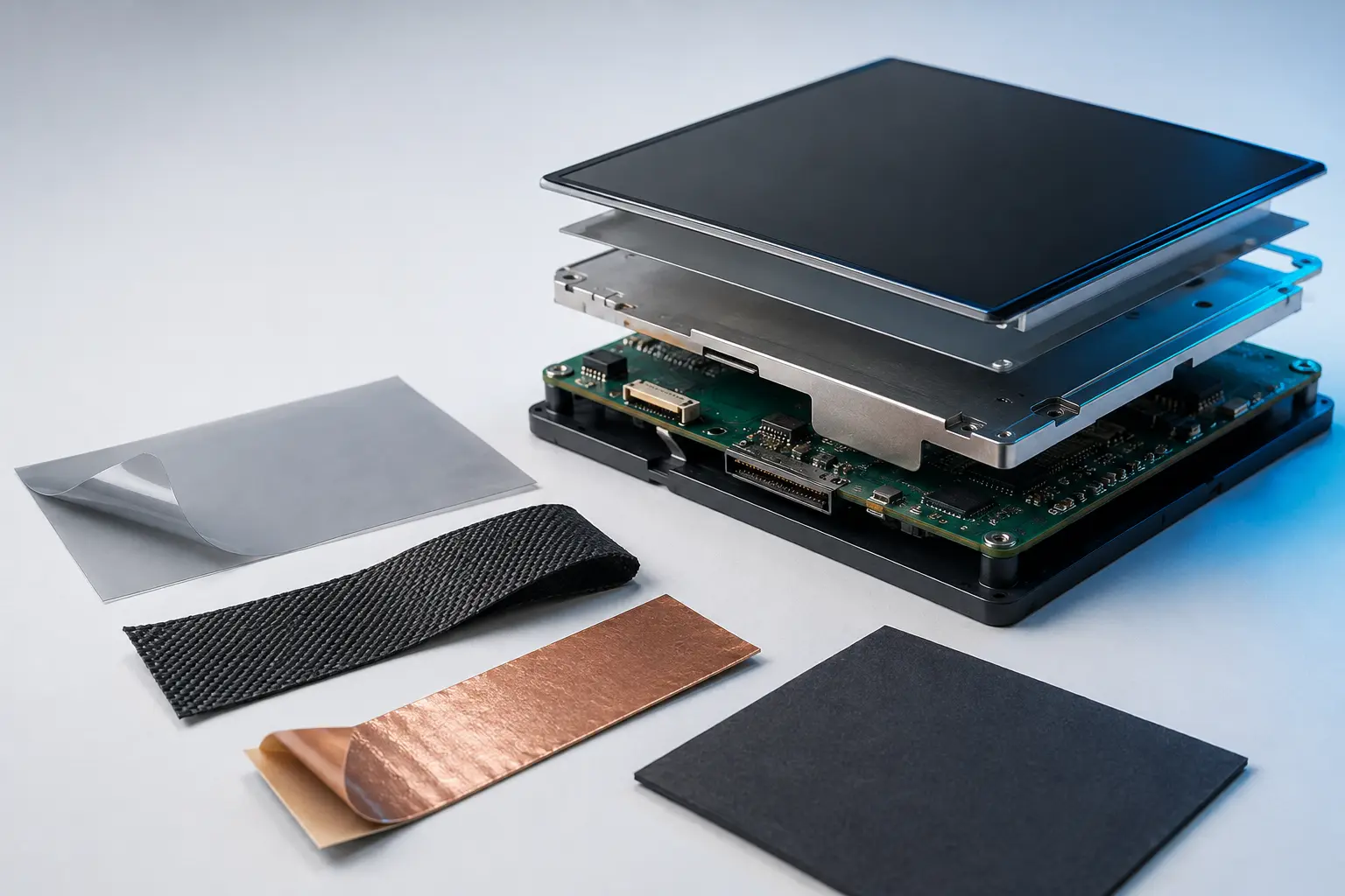
Chaque modèle ECLEAR correspond à un rôle et à une construction distincts. Les correspondances de fabrication restent maîtrisées dans le référentiel produit ECLEAR pour assurer la traçabilité.
Modèle ECLEARProduit / rôleConstruction / plage typeApplications
EC-EM-CF-101Grade du produit10 µm Conductive Adhesive FilmGrade spécifié
Conductive acrylic adhesive film / release liner10 µm; 180° peel >=7 N/25 mm (ASTM D3330); copper-backed XY <0.10 and Z <0.03 Ω/□ tests (GB/T 42909-2023); confirm specimen geometry, load and Z-direction unit before specification
Laminating copper/aluminum foil, conductive fabric and FPC/PCB grounding10 micron conductive adhesive filmconductive PSA
EC-EM-CF-102Grade du produit20 µm Conductive Adhesive FilmGrade spécifié
Conductive acrylic adhesive film / release liner20 µm; 180° peel >=12 N/25 mm (ASTM D3330); copper-backed XY <0.10 and Z <0.03 Ω/□ tests (GB/T 42909-2023); confirm specimen geometry, load and Z-direction unit before specification
Laminating copper/aluminum foil, conductive fabric and FPC/PCB grounding20 micron conductive adhesive filmconductive PSA
EC-EM-CF-103Grade du produit30 µm Conductive Adhesive FilmGrade spécifié
Conductive acrylic adhesive film / release liner30 µm; 180° peel not individually stated N/25 mm (ASTM D3330); copper-backed XY <0.10 and Z <0.03 Ω/□ tests (GB/T 42909-2023); confirm specimen geometry, load and Z-direction unit before specification
Laminating copper/aluminum foil, conductive fabric and FPC/PCB grounding30 micron conductive adhesive filmconductive PSA
EC-EM-CF-104Grade du produit40 µm Conductive Adhesive FilmGrade spécifié
Conductive acrylic adhesive film / release liner40 µm; 180° peel not individually stated N/25 mm (ASTM D3330); copper-backed XY <0.10 and Z <0.03 Ω/□ tests (GB/T 42909-2023); confirm specimen geometry, load and Z-direction unit before specification
Laminating copper/aluminum foil, conductive fabric and FPC/PCB grounding40 micron conductive adhesive filmconductive PSA
EC-EM-CF-105Grade du produit50 µm Conductive Adhesive FilmGrade spécifié
Conductive acrylic adhesive film / release liner50 µm; 180° peel >=15 N/25 mm (ASTM D3330); copper-backed XY <0.10 and Z <0.03 Ω/□ tests (GB/T 42909-2023); confirm specimen geometry, load and Z-direction unit before specification
Laminating copper/aluminum foil, conductive fabric and FPC/PCB grounding50 micron conductive adhesive filmconductive PSA
EC-EM-CF-106Grade du produit100 µm Conductive Adhesive FilmGrade spécifié
Conductive acrylic adhesive film / release liner100 µm; 180° peel >=19 N/25 mm (ASTM D3330); copper-backed XY <0.10 and Z <0.03 Ω/□ tests (GB/T 42909-2023); confirm specimen geometry, load and Z-direction unit before specification
Laminating copper/aluminum foil, conductive fabric and FPC/PCB grounding100 micron conductive adhesive filmconductive PSA
EC-EM-NW-101Grade du produit15 µm Conductive Nonwoven Tape DevelopmentDéveloppement
Conductive acrylic PSA / conductive nonwoven / conductive acrylic PSA / linerDevelopment; 180° peel, A and B: ≥6 N/25 mm (ASTM D3330); XY<0.2 Ω/sq; Z<0.02 Ω/sq; XY/Z retain source notation: confirm the fixture, load, contact area and Z-direction unit before specification
FPC, PCB and antenna grounding
EC-EM-NW-102Grade du produit20 µm Conductive Nonwoven Tape DevelopmentDéveloppement
Conductive acrylic PSA / conductive nonwoven / conductive acrylic PSA / linerDevelopment; 180° peel, A and B: ≥8 N/25 mm (ASTM D3330)
FPC, PCB and antenna grounding
EC-EM-NW-103Grade du produit30 µm Conductive Nonwoven Tape DevelopmentDéveloppement
Conductive acrylic PSA / conductive nonwoven / conductive acrylic PSA / linerDevelopment; 180° peel, A and B: ≥10 N/25 mm (ASTM D3330); XY<0.1 Ω/sq
FPC, PCB and antenna grounding
EC-EM-NW-104Grade du produit50 µm Conformable Conductive Nonwoven Tape DevelopmentDéveloppement
Conductive acrylic PSA / conductive nonwoven / conductive acrylic PSA / linerDevelopment; 180° peel, A and B: ≥12 N/25 mm (ASTM D3330); XY<0.2; Z<0.05 Ω/sq; XY/Z retain source notation: confirm the fixture, load, contact area and Z-direction unit before specification
Curved FPC and PCB grounding
EC-EM-NW-105Grade du produit100 µm Conductive Nonwoven Tape DevelopmentDéveloppement
Conductive acrylic PSA / conductive nonwoven / conductive acrylic PSA / linerDevelopment; 180° peel, A and B: ≥15 N/25 mm (ASTM D3330); Z<0.08 Ω/sq; XY/Z retain source notation: confirm the fixture, load, contact area and Z-direction unit before specification
Gap-bridging conductive bonding
EC-EM-FB-101Grade du produit30 µm Single-Sided Conductive Fabric Tape DevelopmentDéveloppement
Conductive woven fabric / conductive acrylic PSA / linerDevelopment; 180° peel: ≥8 N/25 mm (ASTM D3330); XY<0.1; Z<0.05 Ω/sq; XY/Z retain source notation: confirm the fixture, load, contact area and Z-direction unit before specification
Cable, antenna and camera-module shielding
EC-EM-FB-102Grade du produit50 µm Single-Sided Conductive Fabric Tape DevelopmentDéveloppement
Conductive woven fabric / conductive acrylic PSA / linerDevelopment; 180° peel: ≥10 N/25 mm (ASTM D3330)
Cable, antenna and camera-module shielding
EC-EM-FB-103Grade du produit120 µm Single-Sided Conductive Fabric Tape DevelopmentDéveloppement
Conductive woven fabric / conductive acrylic PSA / linerDevelopment; 180° peel: ≥12 N/25 mm (ASTM D3330); XY<0.2 Ω/sq
EMI wrapping and height compensation
EC-EM-FB-201Grade du produit30 µm Double-Sided Conductive Fabric Tape DevelopmentDéveloppement
Conductive acrylic PSA / woven fabric / conductive acrylic PSA / linerDevelopment; 180° peel, A and B: ≥10 N/25 mm (ASTM D3330); XY<0.1 Ω/sq
FPC grounding and conductive assembly
EC-EM-FB-202Grade du produit50 µm Double-Sided Conductive Fabric Tape DevelopmentDéveloppement
Conductive acrylic PSA / woven fabric / conductive acrylic PSA / linerDevelopment; 180° peel, A and B: ≥12 N/25 mm (ASTM D3330)
FPC grounding and conductive assembly
EC-EM-FB-203Grade du produit100 µm Double-Sided Conductive Fabric Tape DevelopmentDéveloppement
Conductive acrylic PSA / woven fabric / conductive acrylic PSA / linerDevelopment; 180° peel, A and B: ≥15 N/25 mm (ASTM D3330); XY<0.2 Ω/sq
Grounding across moderate gaps
EC-EM-FB-204Grade du produit485 µm Conductive Fabric Spacer Tape DevelopmentDéveloppement
Conductive acrylic PSA / woven fabric spacer / conductive acrylic PSA / linerDevelopment; 180° peel, A and B: ≥18 N/25 mm (ASTM D3330); height-build construction
Large-step grounding and EMI contact
EC-EM-BK-101Grade du produit40 µm Matte-Black Conductive Fabric Tape DevelopmentDéveloppement
Matte-black conductive fabric / conductive acrylic PSA / linerDevelopment; 180° peel: ≥10 N/25 mm (ASTM D3330); conductive black coating
Display shielding and appearance control
EC-EM-BK-102Grade du produit50 µm Matte-Black Conductive Fabric Tape DevelopmentDéveloppement
Matte-black conductive fabric / conductive acrylic PSA / linerDevelopment; 50 µm
Display shielding and appearance control
EC-EM-BK-103Grade du produit50 µm Matte-Black Conductive Copper Tape DevelopmentDéveloppement
Matte-black thermal coating / copper foil / conductive acrylic PSA / linerDevelopment; 180° peel: ≥12 N/25 mm (ASTM D3330); matte heat-spreading coating
Shield cans and speaker modules
EC-EM-BK-104Grade du produit90 µm Black PI/Copper Composite Tape DevelopmentDéveloppement
Matte-black PI single-sided tape / copper foil composite / linerDevelopment; source table marks electrical paths nonconductive; insulating/conformable
Appearance and insulation over copper structures
EC-EM-BK-105Grade du produit25 µm Bright-Black Conductive Copper Tape DevelopmentDéveloppement
Bright-black conductive coating / copper foil / conductive acrylic PSA / linerDevelopment; conductive and alcohol-resistant
Compact EMI shielding with glossy-black appearance
EC-EM-CU-101Grade du produit30 µm Single-Sided Conductive Copper TapeGrade spécifié
Copper foil / conductive acrylic PSA / liner30 µm; 180° peel: ≥10 N/25 mm (ASTM D3330); XY<0.05; Z<0.03 Ω/sq; XY/Z retain source notation: confirm the fixture, load, contact area and Z-direction unit before specification
Grounding, seam shielding and heat spreading30 micron copper foil tape
EC-EM-CU-102Grade du produit50 µm Single-Sided Conductive Copper TapeGrade spécifié
Copper foil / conductive acrylic PSA / liner50 µm; 180° peel: ≥12 N/25 mm (ASTM D3330); XY<0.05; Z<0.03 Ω/sq; XY/Z retain source notation: confirm the fixture, load, contact area and Z-direction unit before specification
Grounding and enclosure shielding50 micron copper foil shielding tape
EC-EM-CU-103Grade du produit45 µm Conformable Single-Sided Copper TapeGrade spécifié
Copper foil / conductive acrylic PSA / liner45 µm; 180° peel: ≥12 N/25 mm (ASTM D3330); low resistance; appearance/conformability control
Shield-can and speaker groundingconformable copper foil tape
EC-EM-CU-104Grade du produit25 µm Double-Sided Conductive Copper TapeGrade spécifié
Conductive acrylic PSA / copper foil / conductive acrylic PSA / liner25 µm; 180° peel, A and B: ≥8 N/25 mm (ASTM D3330); XY<0.05; Z<0.03 Ω/sq; XY/Z retain source notation: confirm the fixture, load, contact area and Z-direction unit before specification
Ultra-thin FPC groundingultra thin double sided copper tape
EC-EM-CU-105Grade du produit20 µm Double-Sided Conductive Copper TapeGrade spécifié
Conductive acrylic PSA / copper foil / conductive acrylic PSA / liner20 µm; 180° peel, A and B: ≥8 N/25 mm (ASTM D3330); XY<0.10; Z<0.05 Ω/sq; XY/Z retain source notation: confirm the fixture, load, contact area and Z-direction unit before specification
Ultra-thin conductive bonding20 micron double sided copper tape
EC-EM-CU-106Grade du produit50 µm Double-Sided Conductive Copper TapeGrade spécifié
Conductive acrylic PSA / copper foil / conductive acrylic PSA / liner50 µm; 180° peel, A and B: ≥8 N/25 mm (ASTM D3330); XY<0.05; Z<0.03 Ω/sq; XY/Z retain source notation: confirm the fixture, load, contact area and Z-direction unit before specification
Conformable grounding and shielding50 micron double sided copper tape
EC-EM-CU-107-DGrade du produitDamp-Heat-Resistant Black/Clear Copper Tape DevelopmentDéveloppement
9 µm clear PSA / 6 µm copper foil / 35 µm black PSA / linerDevelopment; 50±5 µm; dual-85 30-day anti-oxidation target
Long-life humid-heat EMI assemblies
EC-EM-AB-101Grade du produit0-3 GHz EMI Absorber, µ' 50±10Développement
Magnetic-polymer absorber sheet / optional PET double-sided PSA / linerDevelopment; permeability µ'@3 MHz 50±10; absorber thickness options 0.03-0.50 mm
Display backplates, CPU/GPU and wireless-charging noise suppression
EC-EM-AB-102Grade du produit0-3 GHz EMI Absorber, µ' 100±20Développement
Magnetic-polymer absorber sheet / optional PET double-sided PSA / linerDevelopment; permeability µ'@3 MHz 100±20; absorber thickness options 0.03-0.50 mm
Display backplates, CPU/GPU and wireless-charging noise suppression
EC-EM-AB-103Grade du produit0-3 GHz EMI Absorber, µ' 120±20Développement
Magnetic-polymer absorber sheet / optional PET double-sided PSA / linerDevelopment; permeability µ'@3 MHz 120±20; absorber thickness options 0.03-0.50 mm
Display backplates, CPU/GPU and wireless-charging noise suppression
EC-EM-AB-104Grade du produit0-3 GHz EMI Absorber, µ' 150±20Développement
Magnetic-polymer absorber sheet / optional PET double-sided PSA / linerDevelopment; permeability µ'@3 MHz 150±20; absorber thickness options 0.03-0.50 mm
Display backplates, CPU/GPU and wireless-charging noise suppression
EC-EM-AB-105Grade du produit0-3 GHz EMI Absorber, µ' 180±20Développement
Magnetic-polymer absorber sheet / optional PET double-sided PSA / linerDevelopment; permeability µ'@3 MHz 180±20; absorber thickness options 0.03-0.50 mm
Display backplates, CPU/GPU and wireless-charging noise suppression
EC-EM-AB-106Grade du produit0-3 GHz EMI Absorber, µ' 200±20Référence · données à confirmer
Magnetic-polymer absorber sheet / optional PET double-sided PSA / linerLifecycle conflict: present in S08, omitted from S09; permeability µ'@3 MHz 200±20; absorber thickness options 0.03-0.50 mm
Display backplates, CPU/GPU and wireless-charging noise suppression
EC-EM-AB-107Grade du produit0-3 GHz EMI Absorber, µ' 250±20Développement
Magnetic-polymer absorber sheet / optional PET double-sided PSA / linerDevelopment; permeability µ'@3 MHz 250±20; absorber thickness options 0.03-0.50 mm
Display backplates, CPU/GPU and wireless-charging noise suppression
EC-EM-AB-201Grade du produit0.13 High-Frequency EMI Absorber DevelopmentDéveloppement
High-frequency magnetic-polymer absorber / 0.03 mm PSA / linerDevelopment; 1-10 GHz; µ'@3 MHz 40±5; 0.13 mm total: 0.10 absorber + 0.03 PSA
2.4 GHz Wi-Fi, antenna and processor noise suppression
EC-EM-AB-202Grade du produit0.23 High-Frequency EMI Absorber DevelopmentDéveloppement
High-frequency magnetic-polymer absorber / 0.03 mm PSA / linerDevelopment; 1-10 GHz; µ'@3 MHz 40±5; 0.23 mm total: 0.20 absorber + 0.03 PSA
2.4 GHz Wi-Fi, antenna and processor noise suppression
EC-EM-AB-203Grade du produit0.33 High-Frequency EMI Absorber DevelopmentDéveloppement
High-frequency magnetic-polymer absorber / 0.03 mm PSA / linerDevelopment; 1-10 GHz; µ'@3 MHz 40±5; 0.33 mm total: 0.30 absorber + 0.03 PSA
2.4 GHz Wi-Fi, antenna and processor noise suppression
EC-EM-TC-101Grade du produit60 µm Brown Thermosetting Conductive FilmGrade spécifié
Brown thermosetting conductive adhesive film / release liner60 µm before and 40 µm after press; lap resistance ≤1 Ω at Φ = 1.0 mm; no initial tack; validate transfer, hot-press and cure conditions
SMT-reflow-compatible conductive bondingthermosetting conductive adhesive film
EC-EM-TC-102Grade du produit60 µm Black Thermosetting Conductive FilmGrade spécifié
Black thermosetting conductive adhesive film / release liner60 µm before and 38 µm after press; lap resistance ≤2 Ω at Φ = 1.0 mm; no initial tack; validate transfer, hot-press and cure conditions
Black SMT-reflow-compatible conductive bondingblack thermosetting conductive film
EC-EM-TC-103Grade du produit40 µm Brown Thermosetting Conductive FilmGrade spécifié
Brown thermosetting conductive adhesive film / release liner40 µm before and 24 µm after press; lap resistance ≤1 Ω at Φ = 1.0 mm; no initial tack; validate transfer, hot-press and cure conditions
Thin conductive structural bonding40 micron heat cure conductive adhesive
EC-EM-TC-104Grade du produit40 µm Black Thermosetting Conductive FilmGrade spécifié
Black thermosetting conductive adhesive film / release liner40 µm before and 25 µm after press; lap resistance ≤2 Ω at Φ = 1.0 mm; no initial tack; validate transfer, hot-press and cure conditions
Thin black conductive structural bondingblack heat activated conductive film
EC-EM-UV-101-DGrade du produitUV-Curable Gold-Plated Copper Tape DevelopmentDéveloppement
0.05-0.10 µm gold / 9 µm copper / 10 µm UV-conductive adhesive / linerDevelopment; 20±3 µm; low-PIM antenna-feed design
Antenna feedpoint conductive bonding
 ®
®