 ®
®EV Battery & Semiconductor Process Materials
この技術製品群のECLEARモデル、材料構成、用途、プロセスウィンドウ、検証要件をご確認ください。
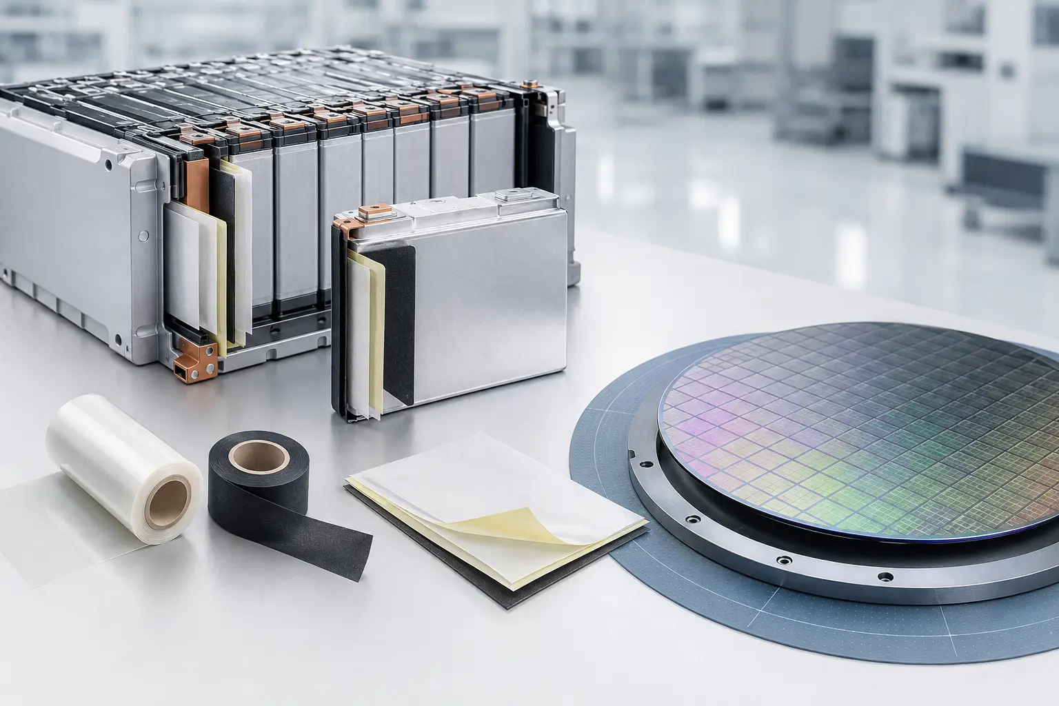
材料積層構造の内容.
各層は機能順に示しており、正確な構成はグレードごとに異なります。
- 01EV: application-specific insulation, flame-retardant, electrode and termination tapes/films
- 02Fuel cell: release liner / silicone adhesive / PEN film
- 03Semiconductor temporary tapes: carrier / responsive PSA / liner by process
- 04Permanent die-attach film: controlled adhesive stack; other thermal-process films: function and removal step require confirmation
技術選定用の個別グレード.
各 ECLEAR モデルは、異なる材料の役割と構成を示します。製造元グレードとの対応情報は、トレーサビリティーのため ECLEAR 製品マスターで管理されます。
Material role must remain explicit across energy and wafer processes.
01EV materials may remain permanently as electrical insulation, flame-control support, fixation, cushioning or structural bonding. Semiconductor materials can be temporary process tapes for grinding, de-taping, dicing and singulation, or permanent films such as selected die-attach materials.
02The same words—film, tape or release—can refer to very different lifecycle roles. Each drawing and process flow must state whether the material remains in the product, how it is activated and at which step it is removed.
03Electrical, thermal, chemical and mechanical performance are stack-level properties. Flame, dielectric, electrolyte, UV-release and wafer-pick claims require a defined standard, thickness, process and final-customer qualification.
用途を基準に評価する性能.
利点は、対象基材、工程、最終アセンブリで評価します。
Clear separation of temporary process films and permanent functional layers
Material families for cell, module, CCS and pack-level needs
Thin PEN-based fuel-cell insulation/fixation option
Process-tape coverage from wafer thinning through package singulation
材料定義から量産積層構造の認定まで.
認定では、材料、加工経路、顧客の生産ラインを一体として確認します。
Permanent insulation/bonding or temporary process support and its removal step.
Set voltage, heat, chemicals, compression, wafer process and activation route.
Freeze thickness, coverage, edge design, dose/heat and equipment settings.
Test electrical, thermal, release, cleanliness and package reliability.
仕様承認前に収集すべき検証データ.
実使用を代表する基材、工程条件、エージング順序を使用してください。
- Dielectric, insulation and edge-coverage evaluation in the EV assembly
- Thermal, flame and chemical testing to the named standard and thickness
- UV or thermal release including shadow, edge and aged conditions
- Wafer breakage, die fly, pick force, residue, low-k and ESD checks
- DAF bondline, void, warpage, cure and package reliability where applicable
数値には試験方法と承認済み改訂版が必要です.
代表値は選定の参考であり、管理規格は承認済み TDS に従います。
代表値は保証規格ではありません。最終基準は承認済みECLEAR TDSとお客様の検証結果に従います。
ライン試験前に技術者が確認する質問.
サンプル依頼前に、材料の役割、界面、工程範囲を明確にしてください。
How are EV and semiconductor material grades specified?+
ECLEAR publishes the applicable family and named grade where the construction is defined. The current controlled TDS then governs thickness, adhesive or film chemistry, process window, packaging and qualification for the intended line.
Can UV-debonding data be transferred between tools?+
No. Spectrum, irradiance, dose uniformity, substrate transmission and shadow areas can change the release result. The customer tool and full process must be validated.
Can ECLEAR recommend a grade from an application description alone?+
A first shortlist is possible, but a production recommendation requires the substrate, layer construction, equipment, process sequence, test method and acceptance criteria. ECLEAR normally moves from requirement definition to laboratory matching, samples, line trial and a frozen approved specification.
Are the values shown on this page guaranteed specifications?+
No. Website values and constructions are selection guidance. Guaranteed limits, test conditions, packaging and shelf life are controlled only by the latest ECLEAR-approved TDS, quality agreement and customer qualification record.
このプラットフォームを評価する用途.
各用途で、積層構造全体の適合性とライン検証が必要です。
管理すべき工程パラメータ.
一つの公称条件だけでなく、工程範囲全体を記録してください。
- Map the material role and removal step in the full process flow.
- Validate electrical, chemical, thermal and aging requirements in the customer stack.
- For process tapes, control dose or thermal activation and shadow/edge zones.
- For permanent films, qualify cure, bondline and package reliability.
選定に必要な情報.
これらの情報により、ECLEAR はグレードと検証計画を絞り込めます。
- Q1Does the material remain in the product or leave during processing?
- Q2What voltage, temperature, flame and chemical environment applies?
- Q3Which process tool, activation route and cycle are used?
- Q4Which regulatory and customer standards control release?
計画的な試験で早期に確認すべきリスク.
早期の不具合確認により、量産拡大のリスクと誤った材料比較を低減します。
Publishing family-level claims as a grade specification
Mixing temporary dicing tape with permanent die-attach film
Incomplete release in shadow areas or after thermal aging
Electrical or chemical failure from stack-level incompatibility
管理された技術文書.
選定した ECLEAR グレードと用途に対応する最新版を請求してください。
代表構成と用途概念は、材料選定のための情報です。供給状況、構成、性能、工程条件はグレードごとに異なり、最新の ECLEAR 承認 TDS、用途試験、および顧客の最終認定に従います。
関連材料システム.
同じ積層構造または工程で本製品と相互作用する周辺材料を確認してください。
単一材料ではなく、積層構造全体を検証してください.
適切な提案のため、基材、構成、工程、合格基準をご提示ください。