 ®
®EV Battery & Semiconductor Process Materials
Energy and semiconductor materials organized by lifecycle role. EV solutions cover insulation, flame control, fixation, sealing and structural bonding. Semiconductor solutions separate temporary grinding, de-taping, dicing, molding-release and singulation materials from permanent die-attach films. Other thermal-process-film roles require confirmation.
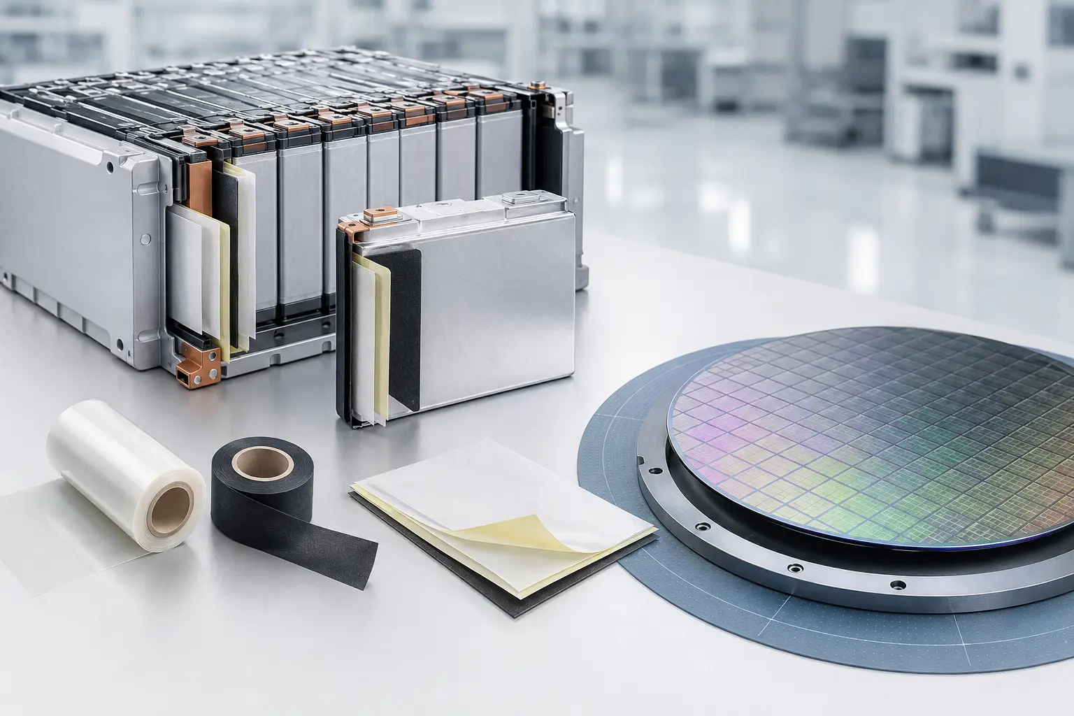
What the material stack contains.
Read the layers in functional order; the exact construction remains grade-specific.
- 01EV: application-specific insulation, flame-retardant, electrode and termination tapes/films
- 02Fuel cell: release liner / silicone adhesive / PEN film
- 03Semiconductor temporary tapes: carrier / responsive PSA / liner by process
- 04Permanent die-attach film: controlled adhesive stack; other thermal-process films: function and removal step require confirmation
Named grades for technical selection.
Each ECLEAR model identifies a distinct material role and construction. Manufacturing cross-references remain controlled in the ECLEAR product master for traceability.
Material role must remain explicit across energy and wafer processes.
01EV materials may remain permanently as electrical insulation, flame-control support, fixation, cushioning or structural bonding. Semiconductor materials can be temporary process tapes for grinding, de-taping, dicing and singulation, or permanent films such as selected die-attach materials.
02The same words—film, tape or release—can refer to very different lifecycle roles. Each drawing and process flow must state whether the material remains in the product, how it is activated and at which step it is removed.
03Electrical, thermal, chemical and mechanical performance are stack-level properties. Flame, dielectric, electrolyte, UV-release and wafer-pick claims require a defined standard, thickness, process and final-customer qualification.
Performance framed around the application.
Benefits are evaluated on the intended substrate, process and finished assembly.
Clear separation of temporary process films and permanent functional layers
Material families for cell, module, CCS and pack-level needs
Thin PEN-based fuel-cell insulation/fixation option
Process-tape coverage from wafer thinning through package singulation
From material definition to a qualified production stack.
Qualification links the material, converting route and customer production line.
Permanent insulation/bonding or temporary process support and its removal step.
Set voltage, heat, chemicals, compression, wafer process and activation route.
Freeze thickness, coverage, edge design, dose/heat and equipment settings.
Test electrical, thermal, release, cleanliness and package reliability.
Evidence to collect before specification release.
Use representative substrates, process conditions and aging sequences.
- Dielectric, insulation and edge-coverage evaluation in the EV assembly
- Thermal, flame and chemical testing to the named standard and thickness
- UV or thermal release including shadow, edge and aged conditions
- Wafer breakage, die fly, pick force, residue, low-k and ESD checks
- DAF bondline, void, warpage, cure and package reliability where applicable
Values require a method and an approved revision.
Typical values support selection; controlled specifications come from the approved TDS.
Typical values are not specifications. Final limits are subject to the approved ECLEAR TDS and customer validation.
Questions engineers ask before a line trial.
Resolve the material role, interfaces and process window before sampling.
How are EV and semiconductor material grades specified?+
ECLEAR publishes the applicable family and named grade where the construction is defined. The current controlled TDS then governs thickness, adhesive or film chemistry, process window, packaging and qualification for the intended line.
Can UV-debonding data be transferred between tools?+
No. Spectrum, irradiance, dose uniformity, substrate transmission and shadow areas can change the release result. The customer tool and full process must be validated.
Can ECLEAR recommend a grade from an application description alone?+
A first shortlist is possible, but a production recommendation requires the substrate, layer construction, equipment, process sequence, test method and acceptance criteria. ECLEAR normally moves from requirement definition to laboratory matching, samples, line trial and a frozen approved specification.
Are the values shown on this page guaranteed specifications?+
No. Website values and constructions are selection guidance. Guaranteed limits, test conditions, packaging and shelf life are controlled only by the latest ECLEAR-approved TDS, quality agreement and customer qualification record.
Where this platform is evaluated.
Each application still requires stack-level compatibility and line validation.
Parameters to control.
Record the complete process window, not only one nominal setting.
- Map the material role and removal step in the full process flow.
- Validate electrical, chemical, thermal and aging requirements in the customer stack.
- For process tapes, control dose or thermal activation and shadow/edge zones.
- For permanent films, qualify cure, bondline and package reliability.
What we need to know.
These inputs allow ECLEAR to narrow the grade and validation plan.
- Q1Does the material remain in the product or leave during processing?
- Q2What voltage, temperature, flame and chemical environment applies?
- Q3Which process tool, activation route and cycle are used?
- Q4Which regulatory and customer standards control release?
What a disciplined trial should expose early.
Early failure checks reduce scale-up risk and prevent false material comparisons.
Publishing family-level claims as a grade specification
Mixing temporary dicing tape with permanent die-attach film
Incomplete release in shadow areas or after thermal aging
Electrical or chemical failure from stack-level incompatibility
Controlled technical documents.
Request the current revision for the selected ECLEAR grade and application.
Typical constructions and application concepts are provided for material selection only. Availability, structure, performance and process conditions are grade-specific and subject to the latest ECLEAR-approved TDS, application testing and final customer qualification.
Related material systems.
Review adjacent materials that interact with this product in the same stack or process.
Validate the complete stack, not one isolated material.
Share the substrate, construction, process and acceptance criteria for a focused recommendation.